TUTORIAL: RFNoC 4 environment development setup for USRP devices
This tutorial is for setting up Radio Frequency Network-on-Chip (RFNoC) version 4 FPGA environment development on universal software radio peripheral (USRP) devices

This tutorial is for setting up Radio Frequency Network-on-Chip (RFNoC) version 4 FPGA environment development on universal software radio peripheral (USRP) devices manufactured by Ettus Research (part of National Instrument). These USRP devices very often are used to capture signals from global navigation satellite system (GNSS) such as global positioning system (GPS), GALILEO, GLONASS, BEIDOU, and others.
USRP device is a general-purpose software define radio (SDR). SDR is a system that performs many of signal processing tasks in a programmable digital signal processing (DSP) engine. This DSP engine, via analog-to-digital (ADC) and digital-to-analog (DAC) circuits, is coupled to analog circuits and then antenna to interface to the air (the communication channel). A detailed explanation of SDR can be found elsewhere.
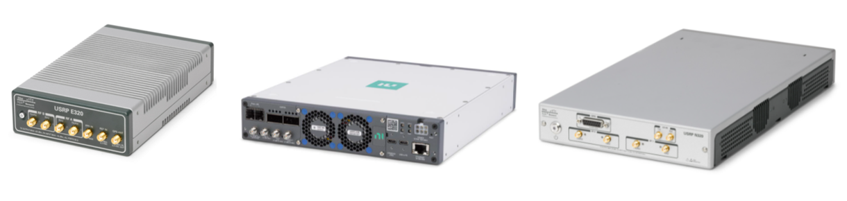
RFNoC is a network-distributed framework of processing tool focusing on enabling FPGA processing in USRP devices. The main goal of RFNoC is to accelerate host-based FPGA development to exploit the power of FPGA computation. The figure below shows several examples of USRP devices that are the three main systems: E,X and N series 3.
The tutorial
Before going thourth the tutorial, there are several important notes:
- Target devices are USRP series 3: X3xx, E3xx and N3xx
- RFNoC 4 is used and is different from the previous RFNoC 3 framework. All FPGA development for USRP series 3 devices should migrate to RFNoC 4. Hence, all RFNoC terms in this document will refer to RFNoC 4.
- This practical guide is unique to RFNoC 4 framework only.
- The term general purpose processor (GPP) and field programmable grid array (FPGA) refers to processing system (PS) and programmable logic (PL), respectively, in Xilinx terminology

1. Introduction
RFNoC is a processing framework to implement a high flexible and high throughput digital signal processing (DSP) in field programmable grid array (FPGA) for software-defined radio (SDR) [1]. RFNoC is implemented for USRP series 3 devices (X3xx, E3xx, N3xx) that are equipped with Xilinx Kintex-7 (X3xx) series or Zynq 7000 series (N3xx, E3xx). The main idea of RFNoC is to handle all inter-blocks communication based on AMBA AXI4 standard and to let users to focus on the design of their HDL logic and to flexibly configure their blocks and the entire FPGA architecture [1,2]. In FPGA, a block refers to an intellectual property (IP) block where a processing logic is implemented in a specific hardware definition languages (HDL), for example Verilog and VHDL [8,9]. All UHD APIs call RFNoC block under the hood.
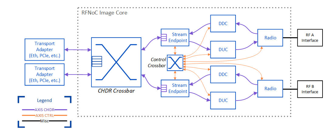
Figure 1 shows the schematic view of the RFNoC framework. In figure 1, the RFNoC framework automatically generates the NoC Core (the dotted box) and the users are responsible for the NoC blocks (the user logic part or user IP block). There are two types of transport among blocks in the framework: data and control transport:
· Data transport
The movement of high-speed and low-latency data among blocks. This transport supports deterministic and timed data streaming with an optional inline metadata inclusion. This data transport needs to be connected via a routing, either a static or dynamic routing, among blocks.
o Dynamic routing: In this routing, the data route among blocks can be reconfigured at run time. However, this configuration require significantly more FPGA resources than static routing.
o Static routing: in this routing, the blocks are statically routed and can only be configured at run time and is not flexible. However, it takes only a significant small resource of FPGA.
· Control transport
The movement of low-speed and high-latency of transactional data such as user register. This type of data can be, for example, block status or control status. There are three types of basic transaction process: register read, register write and bus sleep. All blocks are connected each other for this control transport, via Control Crossbar in figure 1, so that each block can send control message to any blocks. The routing of this control transport can be implemented efficiently in FPGA (because it does not require high throughput and low latency).
· Additional external transport for transporting external data to/from the FPGA (optional).
The NoC core (Figure 1) has four main parts that are:
· CHDR Cross bar
CHDR crossbar is the bus for high throughput and low latency data transport. This bus is set to be 64 bit and designed to support high throughput data stream.
· Stream Endpoint
Stream Endpoint is where all data flows in FPGA section start and end and also as the interface to/from GPP via the Transport blocks. Any IP blocks that are connected to stream endpoint can connect to each other. Connecting IP blocks to stream endpoint is a strategy to make a dynamic routing between blocks where block topologies can be set at will and at run time. However, this dynamic routing strategy require higher significant FPGA resources than static routing strategy.
· Control Crossbar
Control cross bar provide routing from and to all blocks for control transport (user register data). It is automatically constructed by in NoC core. Hence, we can send user register to any block in the FPGA
· Static Router
Static router is to statically connect blocks in the FPGA. All blocks connected via static router have fix routed generated at compile time. This connection is the fastest data route among blocks and requires less FPGA resources than dynamic routing. However, if we want to change the routing configuration among blocks, we need to resynthesise (recompile)the HDL and flash it to the FPGA.

2. Installing RFNoC development framework
To install the RFNoC framework, we need to install a specific version of Vivado, UHD, GNU Radio and Gr-Ettus libraries. The installation should be done in sequence. For RFNoC 4, Ubuntu 20.04-LTS is required. It is recommended that the total free space in the hardrive, where the installation will be carried out, is > 100 GB. Before conducting installation, we need to set the default shell to BASH (by default, the Ubuntu uses DAHS as a default shell) [3] by:
$ sudo dpkg-reconfigure dash
Select “No”, then
$ ll /bin/sh
The installation steps are as follow:
2.0 Installing Dependencies
All required dependencies to install Vivado, UHD, GNU Radio and GR-Ettus need to be installed [4]. Thess dependencies include libtinfo5 and libncurses5 that are required when installing Vivado 2019.1. The installation can be done by:
sudo apt install git cmake g++ libboost-all-dev libgmp-dev swig \
 python3-numpy python3-mako python3-sphinx python3-lxml \
 doxygen libfftw3-dev libsdl1.2-dev libgsl-dev libqwt-qt5-dev \
 libqt5opengl5-dev python3-pyqt5 liblog4cpp5-dev libzmq3-dev \
 python3-yaml python3-click python3-click-plugins python3-zmq \
 python3-scipy python3-gi python3-gi-cairo gobject-introspection \
 gir1.2-gtk-3.0 build-essential libusb-1.0-0-dev python3-docutils \
 python3-setuptools python3-ruamel.yaml python-is-python3 \
 libtinfo5 libncurses5
2.1 Installing Vivado System Suite 2019.1
Before installing Vivado, we need to rename the internet adapter to eth0 (The Xilinx Vivado License Manager looks for an Ethernet adapter with the name “eth0”)[5]:
1. Create files: 70-persistent-net.rules in this directory /etc/udev/rules.d/
2. Adding this line to the file (substitute xx:xx:xx:xx:xx:xx to our MAC address, we can check via ifconfig command):
SUBSYSTEM=="net", ACTION=="add", DRIVERS=="?*", ATTR{address}=="xx:xx:xx:xx:xx:xx", ATTR{dev_id}=="0x0", ATTR{type}=="1", NAME="eth0"3. Then, restart the Linux.
The Vivado version that we need to install is Vivado 2019.1. We reccomned to follyw this video installation [6]. This version of Vivado can be downloaded from Xilinx website [7]. From the website, we can also download the Vivado webpack licence to be able to run the HDL synthesizer for E312.
Note:
· We need to install the System Suite version to be able to run the test bench (Vivado licence is required only when we want to synthesize our HDL)
· For E312, we can use Vivado webpack licence (on the System design suite installation) for free to run the HDL synthesizer and generate the FPGA bit stream file.
2.2 Installing UHD 4
The UHD 4.0 contains the RFNoC framework and can be installed by:
git clone --branch UHD-4.0 https://github.com/ettusresearch/uhd.git   uhd
mkdir uhd/host/build; cd uhd/host/build
cmake ..
make
sudo make install
2.3 Installing GNU Radio 3.8
The GNU Radio 3.8 can be installed by:
git clone --branch maint-3.8 --recursive   https://github.com/gnuradio/gnuradio.git gnuradio
mkdir gnuradio/build; cd gnuradio/build;
cmake ..
make
sudo make install
2.4 Installing Gr-Ettus
Gr-Ettus is required especially if we want to integrate our RFNoC to GNU Radio Companion (GRC) only. However, even if we do not want to integrate our RFNoC into GRC, we still require to install this library to use rfnocmodtool (a python based software) to create our RFNoC development environment. rfnocmodtool is a tool to create RFNoC development project folder and skeleton project files. Gr-Ettus can be installed by:
git clone --branch maint-3.8-uhd4.0  https://github.com/ettusresearch/gr-ettus.git gr-ettus
mkdir gr-ettus/build; cd gr-ettus/build;
cmake -DENABLE_QT=True ..
make
sudo make install
Note:
· Installing GNU Radio and Gr-Ettus are still required even though we will not use GNU Radio Companion integration. However, this GNU Radio is required for Gr-Ettus and Gr-Ettus is required for rfnocmodtool.
3. Creating RFNoC development environment
To create the RFNoC development environment, that is to create project and skeleton files, we use rfnocmodtool. To use rfnocmodtool in a shell terminal, we need to export the rfnocmodtool path in the terminal environment:
export PYTHONPATH=/usr/local/lib/python3/dist-packages/:$PYTHONPATH
then,
sudo ldconfig
to cretae a new RFNoC module (new project), it can be done by:
rfnocmodtool newmodinsert a “ProjectName” and it will crete a folder “rfnoc-ProjectName” in the active directory.
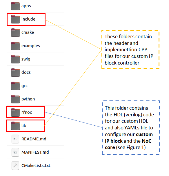
Figure 2 shows the created project folder of an RFNoC development after running rfnocmodtool newmod. In Figure 2, there are three most relevant folder for the RFNoC development: rfnoc, include and lib folders. The rfnoc foldercontains all necessary folder to create our own custom IP block and to configure our custom block and RFNoC code. The custom IP block is by a genertaed skeleton verilog and the test bench file is by a generated system verilog files. Meanwhile, the include and lib folders contain the header and implemnetation C++ file for our custom block controller to access our block via C++ UHD API.
Figure 3 shows autogenerated sub-project folders inside the rfnoc folder (Figure 2). There are three sub-folders: blocks, fpga and icores folders. The blocks folder contains the YAML file to configure our custom IP blocks and the icores folder contains the YAML file to configure NOC core in the developped RFNoC. Finally, fpga folder contains the autogenerated FPGA block folder (the folder name format is rfnoc_block_BLOCKNAME). This FPGA block folder contains skeleton files for our custom IP blocks where user logic is in verilog and user test bench is in system verilog. Initially, the fpga folder contains no FPGA block folder until we create our custom block development, that is, adding new NOC block into a developped RFNoC.
To add a new custom NOC block (FPGA block), go to the created RFNoC project folder. It can be done by:
cd rfnoc-ProjectNameand then type
rfnocmodtool addinsert the “BlockName” and it will create a rfnoc_block_BlockName folder in rfnoc folder (Figure 2).
Note:
· To see all possible rfnocmodtool command options, type
rfnocmodtool help
· To remove a custom NOC block (custom IP block), we can use command rfnocmodtool remove
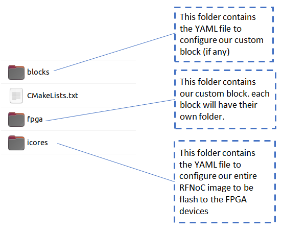
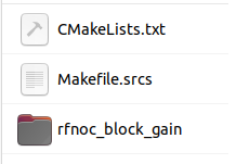
Figure 4 shows an example of an auto generated sub-project folder when we create a new custom IP block called gain by using rfnocmodtool add command. Hence, the sub-project folder created in the fpga folder (please see figure 3) is rfnoc_block_gain. Inside this block, there will be three auto generated files for custom user logic implementation (in Verilog), user test bench (in System Verilog) and NOC shell for the custom IP block (in Verilog). In this example, the user logic file is rfnoc_block_gain.v, the user test bench is rfnoc_block_gain_tb.sv and the NOC shell file is noc_shell_gain.v (note that “gain” is the name of the custom block that we have created before).
4. Customised IP block development
The development of custom IP block focuses on HDL files (verilog and system verilog) inside block folders in the fpga folder (figure 3) and YAML files, each corresponds to created custom blocks, inside the block folder (figure 3). We will discuss the YAML file configuration later on in the RFNoc development section.
Commonly, we just focus on the YAML files (BLOCK_NAM.yml), rfnoc_block_BLOACK_NAME.v and rfnoc_block_BLOCK_NAME_tb.sv. The noc_shell_BLOCK_NAME.v can be modified if we want to customise the data transport behaviour from and to our custom IP block (which is mostly not carried out in most scenarios).
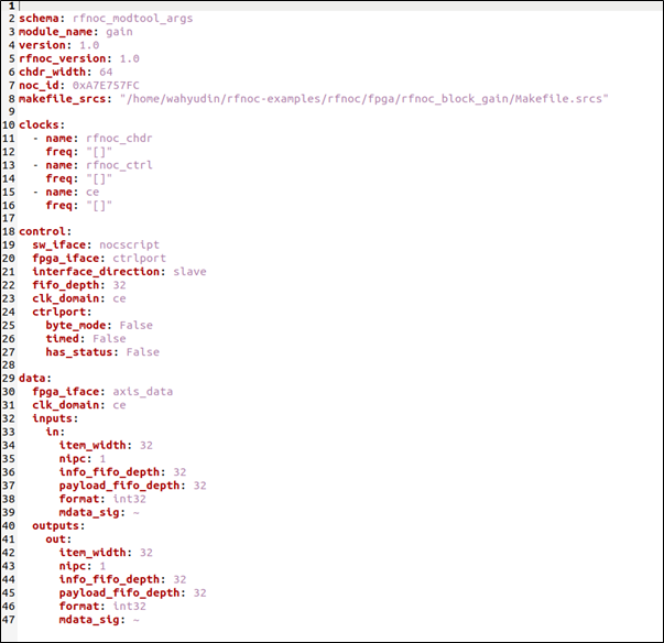
Figure 5 shows an example of the YAML file of a gain block created by rfnocmodtool add. Explanations for an example YAMl file in figure 5 are as follows (refer to [1]). The NOC id is auto generated when we created the block. However, we can insert the id manually. chdr_width is the bit width for the CHDR crossbad (figure 1).
The clock section contains the name of the clocks that are required in the block and will be used to connect from clock sources. rfnoc_chdr and rfnoc_ctrl are required clock name (the name cannot be changed) and ce is user defined clock (the name can be changed). Also, we can set the acceptable range of the operating clock for each clock name. the main sections are control and data sections. Controlcontains the options or settings fo rthe control bus and data contains the options or settings for data bus, including number and name of input and output ports in the block.
Additional sections (not shwon in this example) for advance feature are io_port section for external block communication with external I/Os, registers section for listing all additional user registers (on top of one default user regster set when we cretae dthe block) in the block and properties section for listing all block user properties.
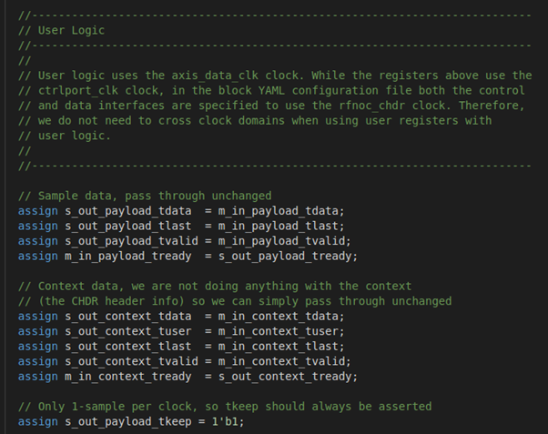
To start developing our custom logic, we can insert our logic into rfnoc_block_BLOCK_NAME.v file. Figure 6 shows the section of in the verlilog file where we can insert our own user logic to develop a custom IP block. This user lofic section is at the end of the verilog file. There are default variables generated in the file, that are variable for user sample data and context data. In most cases, it is the sample data that we want to process with our own logic, for example multiply input sample data with a specific gain value to create a modifed output sample data. The input sample data variable is m_in_payload_tdata and the output data variable is s_out_payload_tdata (“m” refers to master and “s” refers to slave to match Xilinx terminology [9]).
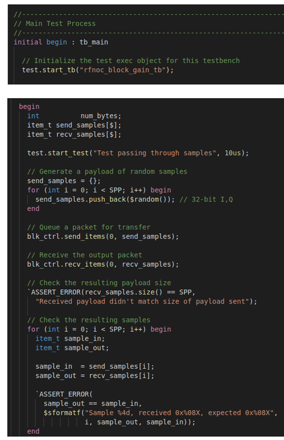
To test our user logic, we can modify the rfnoc_block_BLOCK_NAME_tb.sv file. Figure 7 shows the auto generated skeleton test bench file. To insert our own test logic, we can edit or insert code in the Main Test Process section (as shown in figure 7). In this test section, there are several default test code generated by the rfnocmodtool when we create or add a block. Each test logic in the main test process section is inside begin and end section.
It is worth to note that, in some situations, it may be difficult if not impossible to insert our custom test logic in the test bench. In this situation, we may skip the test and do not need to edit or modify the default test file.
The next step is to build (compile and run) the user logic Verilog file and test bench system Verilog file. To do the build process, we create a build folder inside the generated project folder (the project folder name format is rfnoc-MOUDLE_NAM). From this build folder, we type:
cmake -DUHD_FPGA_DIR=~/uhd/fpga ..This command assumes that the RFNoC project folder, generated by command rfnocmodtol newmod, is in Home directory (~). After building process, we can compile and run the user logic and test bench files and synthesise the RFNoC image (NOC core as shown in figure 1).
Note that after running “cmake -DUHD_FPGA_DIR=~/uhd/fpga ..”, we only do make and make install if we want to integrate to GNC software. It will compile to libgnuradio-PROJECTNAME.so and some python *.pyc and *.pyo files and some other files, eg. SWIG, etc required for GRC integration.
To compile the Verilog code (HDL) and run the test bench [8,9] (to test the logic of our custom block), from the build folder, type:
make rfnoc_block_BlockName_tbthis command will compile both the user logic and test bench files and run the test bench. Any compile errors found form the user logic Verilog files will be shown in the results of the command.
5. Customised RFNoC image development
Finally, after developing our custom IP block containing our own user logic, we will insert the custom block into the general RFNoC configuration. This RFNoC configuration will be synthesised and flashed to USRP series 3 devices. In this step, we also configure the routing of the block in the NOC core, either statically (less FPGA resource and less flexible) or dynamically (more FPGA resource and more flexible). Also, we need to connect the clock domain source to NOC blocks in the RFNoC configuration.
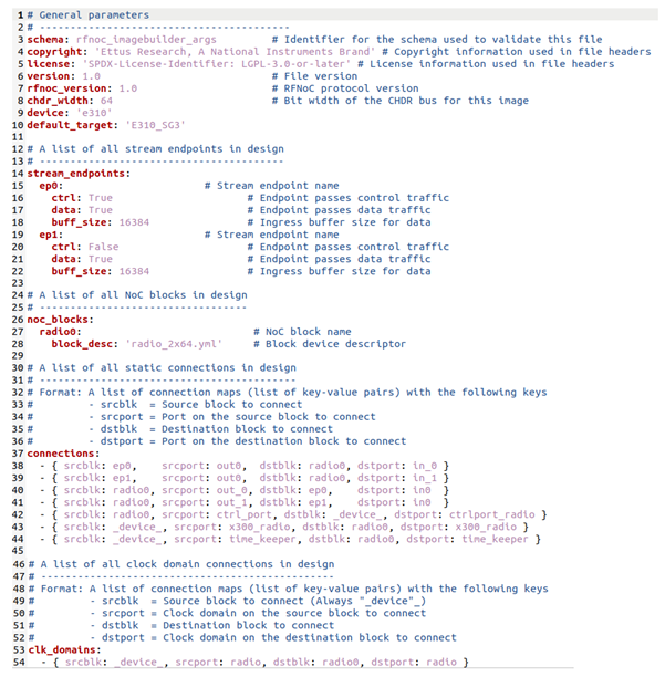
To develop and configure the RFNoC, we modify the FILENAME_rfnoc_image_core.yml file that is generated by the rfnocmodtool newmod command. Figure 8 shows a typical YAML file for the RFNoC development. The explanations of the YAML file are as follows. We can add stream end points in the stream endpoints and NOC blocks (either default block from UHD or our custom blocks) in the list of noc_blocks section. In the list of connections section, we configure the routing of our block either statically or dynamically. Static routing is route explicitly mention in this static connection section. However, to make the routing dynamic, we must create a static connection from a stream endpoint to a NOC block and form this NOC block back to the stream endpoint. Since, everything connected to the stream endpoint can connect to any stream endpoint via the CHDR crossbar (figure 1), then, by this strategy we create a dynamic connection among blocks (please see section 1). It is worth to note that creating this “dynamic” connections will require a significantly more FPGA resources than the straightforward static routing (in some cases we may not fit the RFNoC image into a USRP FPGA device). Finally, in the clk_domains section, we connect clock sources to all NOC blocks in the RFNoC configuration.
NOTE: to be able to generate this xxx_rfnoc_image_code, we need to at least creat one rfnoc block with rfnocmodtool add command eventhough if we do not use this block
To synthesis the developed RFNoC block, from the build folder:
make FILENAME_rfnoc_image_coreThis synthesis process will take some time (typically one hour depending on the CPU resource). I this step, the size of our RFNoC development will be compared with the FPGA capacity of a target USRP device. If the RFNoC size is more than the FPGA capacity, then an error will occur. In addition, this synthesis step also shows errors if there is a logic error in our user logic verilog code.
When successful, the synthesised bit stream (the RFNoC image) is generated in UHDInstallPath/uhd/fpga/usrp3/top/x3xx/build Where UHDInstallPath is the path of the UHD installation (commonlyHome) and x3xxis the type of the USRP 3 devise we use.
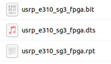
Figure 9 shows an example of the build results. There are three files with extension *.bit, *. dts, *. rpt. The *.bit file is the bit stream file containing the binary of an RFNoC image. The other two files are also required when we load the image to a target device (these two *. dts and *. rpt files need to always be present in the same folder of the *.bit file for loading process).
6. Loading the customised RFNoC image to an USRP device
Finally, after a successful synthesis process of our RFNoC image development, we need to load the synthesis image (the bit stream file) to a target USRP devices.
For E312 (assuming we are in the folder containing the *.bit file):
uhd_image_loader –-args=”type=e3xx” –-fpga-path=./filename.bitTo check whether the synthesis RFNoC image is successfully loaded into the target ISRP device, type:
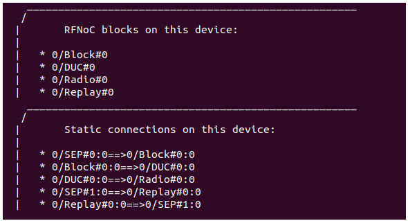
uhd_usrp_probeFigure 10 shows an example of successful flashing of an RFNoC image into a e312 USRP device. In Figure 10, all the NOC blocks included in the icore YAML file (figure 8) and their connections are shown.
It is worth to note that, although when our custom RFNoC image (the bit file) can be synthesised, if there is a mistake or fault in the RFNoC configuration (that violates the RFNoC framework rules), the uhd_usrp_probe will output error during the probing process.
References
[1] RFNoC 4 Specification version 1 https://files.ettus.com/app_notes/RFNoC_Specification.pdf
[2] Getting Started with RFNoC in UHD 4.0 https://kb.ettus.com/Getting_Started_with_RFNoC_in_UHD_4.0
[3] Getting Started with RFNoC Development https://kb.ettus.com/Getting_Started_with_RFNoC_Development
[4] RFNoC 4 Migration Guide https://kb.ettus.com/RFNoC_4_Migration_Guide
[5] RFNoC https://kb.ettus.com/RFNoC
[6] Youtube video on how to install Xilinx Vivado https://www.youtube.com/watch?v=iwVd4TIB0ME&t=1525s
[7] Xilinx Vivado 2019.1 https://www.xilinx.com/support/download/index.html/content/xilinx/en/downloadNav/vivado-design-tools/archive.html
[8] Ünsalan, C. and Tar, B., 2017. Digital system design with FPGA: implementation using Verilog and VHDL. McGraw-Hill Education.
[9] Crockett, L.H., Elliot, R., Enderwitz, M. and Stewart, R., 2014. The Zynq Book: Embedded Processing with the Arm Cortex-A9 on the Xilinx Zynq-7000 All Programmable Soc. Strathclyde Academic Media.
We sell all the source files, EXE file, include and LIB files as well as documentation of ellipse fitting by using C/C++, Qt framework, Eigen and OpenCV libraries in this link.
We sell tutorials (containing PDF files, MATLAB scripts and CAD files) about 3D tolerance stack-up analysis based on statistical method (Monte-Carlo/MC Simulation).